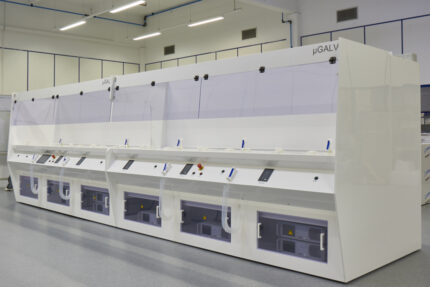


Porous Silicon Formation µPORSI
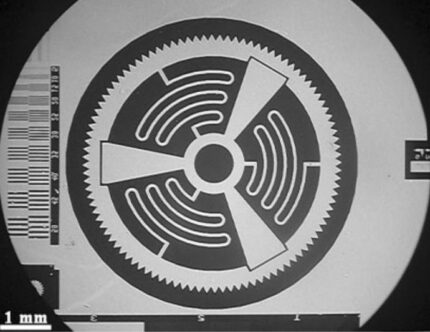
Current application area’s are LED, Photovoltaics and Semiconductor. Porous silicon (PS) is a material formed by anodic dissolution of single crystalline silicon in HF containing solutions.
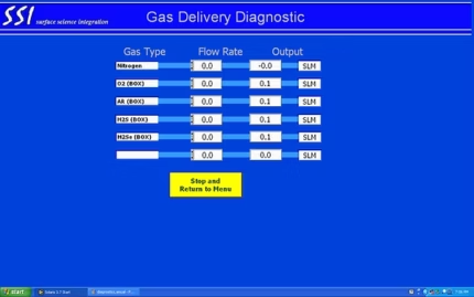
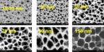
The concentration of the electrolyte in the pores of µPorSi is constant during anodization and the anodic reaction in the pores proceeds uniformly in the thickness direction. The dissolution of silicon in the pores is the results of the divalent and the tetravalent reactions of silicon with , without the disproportionation reaction. The insoluble surface porous film (SPF) exists at the surface of µPorSi and the silicic acid is formed in µPorSi.
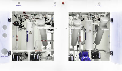
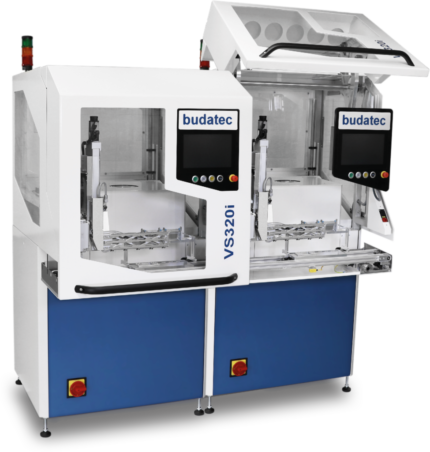
MOT offers the complete production process including drying, the system µPorSi is dedicated for the production of porous Silicon. As support we offer the process ramp-up at customer site.
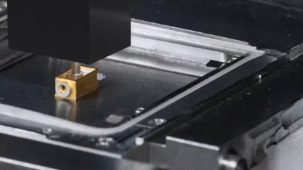
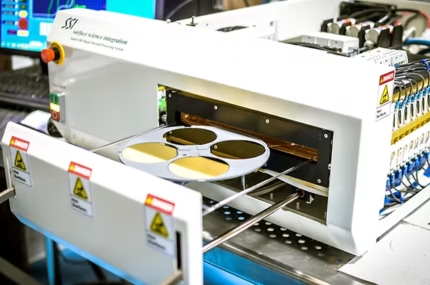
Customized solution in terms of process flow including hanling and in terms of wafer sizes are possible.