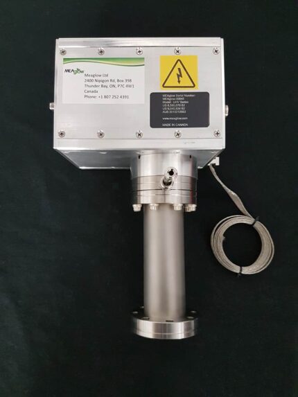
Series 16 Hollow Cathode
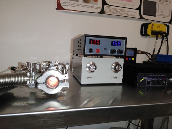
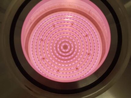
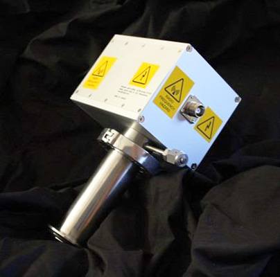
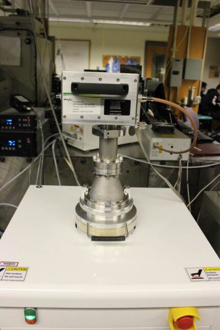
The Series 16 is the result of a mini plasma source developed for NASA Goddard. This version is based on NW 16 fittings. The Series 16 is a compact alternative suitable for small research systems. A low cost RF power supply solution can also be supplied by Meaglow Ltd. This includes a 13.56 MHz pre amplifier (27.12 MHz is also possible), a linear amplifier, a power meter and manual match box, plus cabling.
- Max. 80 watt operation continuously, up to 100 watt in pulse mode.
- No water cooling. The system can get hot and present a heat hazard, air cooling can moderate this.
- Suitable for 2 to 4” wafers and smaller test samples.
- Oxides, nitrides, other.
- Hollow Cathode Technology with Low oxygen contamination.
- Cost effective.
- High density of up to 10 12 cm 3 or higher dependent on conditions.
- Wide range of operating pressures (eg. from <200 mTorr to >10 Torr).
- Improved growth per cycle for many material systems.
Related Papers:
- C. Ozgit-Akgun, E. Goldenberg, A. Kemal Okyay and N. Biyikili, Journal of Materials Chemisty C 2 (2014) 2123.
- K.S. A. Butcher, V Georgiev and D. Georgieva, Coatings 11 (2021) 1506.
HOLLOW CATHODE ALD PAPERS
• Growth of conformal TiN thin film with low resistivity and impurity via hollow cathode plasma atomic layer deposition
H. Y. Lee, J. H. Han and B. J. Choi
J. Vac. Sci. Technol. A 42 (2024) 022405.
• High-quality SiNx thin-film growth at 300 degree C using atomic layer deposition with hollow-cathode plasma
J. C. Park, D. H. Kim, T. J. Seok, D. W. Kim, J.-H. Ahn, W.-H. Kim and T. J. Park
J. Mater. Chem. C. 11 (2023) 9107.
• Low-temperature synthesis of crystalline vanadium oxide films using oxygen plasmas
A. Mohammad, K. D. Joshi, D. Rana, S. Ilhom; B. Wells, B. Willis, B Sinkovic, A. K. Okyay and N. Biyikli
J. Vac.Sci. Technol. A 41 (2023) 032405.
• Reducing the β‑Ga2O3 Epitaxy Temperature to 240 °C via Atomic Layer Plasma Processing
S. Ilhom, A. Mohammad, J. Grasso, B. G. Wil,is, A. K. Okyay, and N. B.iyikli
ACS Appl. Electron. Mater. 5 (2023) 335.
• Hollow cathode enhanced capacitively coupled plasmas in Ar/N2/H2 mixtures andimplications for plasma enhanced ALD
D. R. Boris, M. J. Johnson, C. R. Eddy and S. G. Walton
J. Vac. Sci. Technol. B 40 (2022) 044002.
• Erratum: ‘‘Hollow cathode enhanced capacitively coupled plasmas in Ar/N2/H2 mixtures and implications for plasma enhanced ALD” [J. Vac. Sci. Technol. B 40, 044002 (2022)]
D. R. Boris, M. J. Johnson, C. R. Eddy and S. G. Walton
J. Vac. Sci. Technol. B 40 (2022) 057001.
• Atomic Layer Deposition for Thin Film Solid‑State Battery and Capacitor
Dohyun Go, Jeong Woo Shin, Seunghyeon Lee, Jaehyeong Lee, Byung Chan Yang, Yoonjin Won, Munekazu Motoyama, and Jihwan An
Int. J. of Precis. Eng. and Manuf.-Green Tech. (2022).
• Synthesis And Characterization of Platinum on Carbon Nanoparticles Selectively Coated with Titanium Nitride (TiN)
Andres O. Godoy, Saidjafarzoda Ilhom, Mor Kattan, Pablo Zarama, Yair Ein-Eli, Necmi Biyikli, and Jasna Jankovi
ECS Trans. 104 (2021) 29.
• Controlling and Optimizing Photoinduced Charge Transfer across Ultrathin Silica Separation Membrane with Embedded Molecular Wires for Artificial Photosynthesis
Hongna Zhang, Ian Weiss, Indranil Rudra, Won Jun Jo, Simon Kellner, Georgios Katsoukis, Elena Galoppini, and Heinz Frei
ACS Appl. Mat. Interfaces 13 (2021) 23532.
• Recent Advances in Hollow Cathode Technology for Plasma-Enhanced ALD—Plasma Surface Modifications for Aluminum and Stainless-Steel Cathodes
K.S.A. Butcher, V. Georgiev and D. Georgieva
Coatings 11 (2021) 1506.
• Low-Temperature As-Grown Crystalline β‑Ga2O3 Films via Plasma-Enhanced Atomic Layer Deposition
Saidjafarzoda Ilhom, Adnan Mohammad, Deepa Shukla, John Grasso, Brian G. Willis, Ali Kemal Okyay and Necmi Biyikli
ACS Appl. Mater. Interfaces 13 (2021) 8538.
• Plasma-Enhanced Atomic-Layer Deposition of Nanometer-Thick SiNx Films Using Trichlorodisilane for Etch-Resistant Coatings
Su Min Hwang, Harrison Sejoon Kim, Dan N. Le, Arul Vigneswar Ravichandran, Akshay Sahota, Jaebeom Lee, Yong Chan Jung, Si Joon Kim, Jinho Ahn, Byung Keun Hwang, Lance Lee, Xiaobing Zhou, and Jiyoung Kim
ACS Appl. Nano. Mater. 4 (2021) 2558.
• Real-time in situ process monitoring and characterization of GaN films grown on Si (100) by low-temperature hollow-cathode plasma-atomic layer deposition using trimethylgallium and N2/H2 plasma
Deepa Shukla, Adnan Mohammad, Saidjafarzoda Ilhom, Brian G. Willis, Ali Kemal Okyay and Necmi Biyikli
J. Vac. Sci. Technol. A 39 (2021) 022406.
• High-Temperature Atomic Layer Deposition of GaN on 1D Nanostructures
A. J. Austin, E. Echeverria, P. Wagle, P. Mainali, D. Meyers, A. K. Gupta, R. Sachan, S. Prassana and D. N. McIlroy
Nanomaterials 10 (2020) 2434.
• Chemical vapor deposition of metallic films using plasma electrons as reducing agents
Hama Nadhom, Daniel Lundin, Polla Rouf, and Henrik Pedersen
J. Vac. Sci. Technol. A 38 (2020) 033402.
• Elucidating the role of nitrogen plasma composition in the low-temperature self-limiting growth of indium nitride thin films
Saidjafarzoda Ilhom, Adnan Mohammad, Deepa Shukla, John Grasso, Brian G. Willis, Ali K. Okyay and Necmi Biyikli
RSC Adv. 10 (2020) 27357.
• The role of plasma in plasma-enhanced atomic layer deposition of crystalline films
David R. Boris, Virginia D. Wheeler, Neeraj Nepal, Syed B. Qadri, Scott G. Walton, and Charles (Chip) R. Eddy
J. Vac. Sci. Technol. A 38 (2020) 040801.
• High growth rate and high wet etch resistance silicon nitride grown by low temperature plasma enhanced atomic layer deposition with a novel silylamine precursor
Harrison Sejoon Kim, Su Min Hwang, Xin Meng, Young-Chul Byun, Yong Chan Jung, Arul Vigneswar Ravichandran, Akshay Sahota, Si Joon Kim, Jinho Ahn, Lance Lee, Xiaobing Zhou, Byung Keun Hwange and Jiyoung Kim
J. Mater. Chem. C 8 (2020) 13033.
• Understanding the role of rf-power on AlN film properties in hollow-cathode plasma-assisted atomic layer deposition
Saidjafarzoda Ilhom, Deepa Shukla, Adnan Mohammad, John Grasso, Brian Willis and Necmi Biyikli1
J. Vac. Sci. Technol. A 38 (2020) 022406.
• Effect of N2/H2 plasma on the growth of InN thin films on sapphire by hollow-cathode plasma-assisted atomic layer deposition
Mustafa Alevli and Nese Gungor
J. Vac. Sci. Technol. A 38 (2020) 062407.
• Review—Silicon Nitride and Silicon Nitride-Rich Thin Film Technologies: State-of-the-Art Processing Technologies, Properties, and Applications
A. E. Kaloyeros, Y. Pan, J. Goff and B. Arkles
ECS Journal of Solid State Science and Technology 9 (2020) 063006.
• Low-temperature atomic layer deposition of high quality SiO2 and Si3N4 thin films
PhD Thesis, Dr. Dae Hyun Kim, Graduate School of Hanyang University, August 2019.
• Hollow cathode plasma (HCP) enhanced atomic layer deposition of silicon nitride (SiNx) thin films using pentachlorodisilane (PCDS)
Su Min Hwang, Aswin L. N. Kondusamy, Qin Zhiyang, Harrison Sejoon Kim, Xin Meng, Jiyoung Kim, Byung Keun Hwang, Xiaobing Zhou, Michael Telgenhoff and Jeanette Young
ECS Trans. 89 (2019) 63.
• Visible/infrared refractive index and phonon properties of GaN films grown on sapphire by hollow-cathode plasma-assisted atomic layer deposition.
Nese Gungor and Mustafa Alevi.
J. Vac. Sci. Technol. A 37 (2019) 050901
• Real-time in situ ellipsometric monitoring of aluminum nitride film growth via hollow cathode plasma-assisted atomic layer deposition.
Adnan Mohammad, Deepa Shukla, Saidjafarzoda Ilhom, Brian Willis, Blaine Johs, Ali Kemal Okyay, and Necmi Biyikli.
J. Vac. Sci. Technol. A 37 (2019) 020927.
• Investigation of the Physical Properties of Plasma Enhanced Atomic Layer Deposited Silicon Nitride as Etch Stopper.
Harrison Sejoon Kim, Xin Meng, Si Joon Kim, Antonio T. Lucero, Lanxia Cheng, Young-Chul Byun, Joy S. Lee, Su Min Hwang, Aswin L. N. Kondusamy, Robert M. Wallace, Gary Goodman, Alan S. Wan, Michael Telgenhoff, Byung Keun Hwang, and Jiyoung Kim
ACS Applied Materials and Interfaces 10 (2018) 44825.
• Emergent Electrical Properties of Ensembles of 1D Nanostructures and Their Impact on Room Temperature Electrical Sensing of Ammonium Nitrate Vapor
Lyndon D. Bastatas, Elena Echeverria-Mora, Phadindra Wagle, Punya Mainali, Aaron Austin, and David N. McIlroy
ACS Sensors 3 (2018) 2367.
• Fabrication of Core−Shell Nanotube Array for Artificial Photosynthesis Featuring an Ultrathin Composite Separation Membrane.
E. Edri, S. Aloni, and H. Frei
ACS Nano 12 (2018) 533.
• Nanoscale membranes that chemically isolate and electronically wire up the abiotic/biotic interface.
J. A. Cornejo, H. Sheng, Eran Edri, C. M. Ajo-Franklin and H. Frei
Nature Communications 9 (2018) 2263.
• Robust SiNx/GaN MIS-HEMTs with Crystalline Interfacial Layer Using Hollow Cathode PEALD
X. Meng, J. Lee, A. V. Ravichandran, Y.-C. Byun, J.-G. Lee, A. T. Lucero, S. J. Kim, M.-W Ha, C. D. Young and J. Kim
IEEE Electron Device Letters 39 (2018) 1195.
• Hollow Cathode Plasma-Enhanced Atomic Layer Deposition of Silicon Nitride Using Pentachlorodisilane.
X. Meng, H. S. Kim, A. T. Lucero, S. M. Hwang, J. S. Lee, Y.-C. Byun, J. Kim, B. K. Hwang, X. Zhou, J. Young and M. Telgenhoff
ACS Applied Materials and Interfaces 10 (2018) 14116.
• Long-Range Ordered Vertical III-Nitride Nano-cylinder Arrays via Plasma-Assisted Atomic Layer Deposition.
A. Haider, P. Deminskyi, M. Yilmaz, K. Elmabruk, I. Yilmaz and N. Biyikli
Journal of Materials Chemistry C, 6 (2018) 6471.
• Influence of N2/H2 and N2 plasma on binary III-nitride films prepared by hollow-cathode plasma-assisted atomic layer deposition.
Mustafa Alevli, and Nese Gungor
Journal of Vacuum Science and Technology A36 (2018) 01A110.
• Graphene as a plasma-compatible blocking layer material for area-selective atomic layer deposition: a feasibility study for III-nitrides.
Petro Deminskyi, Ali Haider, Evgeniya Kovalska and Necmi Biyikli
Journal of Vacuum Science and Technology A36 (2018) 01A107.
• Atomic layer deposition: an enabling technology for the growth of functional nanoscale semiconductors.
Necmi Biyikli and Ali Haider
Semicond. Sci. Technol. 32 (2017) 093002.
• Demonstration of flexible thin film transistors with GaN channels.
S. Bolat, Z. Sisman, and A. K. Okyay
Applied Physics Letters 109 (2016) 233504.
• Substrate impact on the low-temperature growth of GaN thin films by plasma-assisted atomic layer deposition.
Seda Kizir, Ali Haider, and Necmi Biyikli
Journal of Vacuum Science and Technology A34 (2016) 041511.
• Low-temperature self-limiting atomic layer deposition of wurtzite InN on Si(100)
Ali Haider, Seda Kizir, and Necmi Biyikli
AIP Advances 6 (2016) 045203.
• Comparison of trimethylgallium and triethylgallium as “Ga” source materials for the growth of ultrathin GaN films on Si (100) substrates via hollow-cathode plasmaassisted atomic layer deposition.
Mustafa Alevli, Ali Haider, Seda Kizir, Shahid A. Leghari, and Necmi Biyikli
Journal of Vacuum Science & Technology A 34 (2016) 01A137.
• Substrate temperature influence on the properties of GaN thin films grown by hollow cathode plasma-assisted atomic layer deposition.
Mustafa Alevli, Neşe Gungor, Ali Haider, Seda Kizir, Shahid A. Leghari, and Necmi Biyikli
Journal of Vacuum Science & Technology A 34 (2016) 01A125.
• Low-temperature sequential pulsed chemical vapor deposition of ternary BxGa1-xN and BxIn1-xN thin film alloys.
Ali Haider, Seda Kizir, Cagla Ozgit-Akgun, Ali Kemal Okyay, and Necmi Biyikli
Journal of Vacuum Science & Technology A 34 (2016) 01A123.
• Charge Transport through Organic Molecular Wires Embedded in Ultrathin Insulating Inorganic Layer.
E. Edri and H. Frei
Journal of Physical Chemistry C 119 (2015) 28326.
• Hollow-Cathode Plasma-Assisted Atomic Layer Deposition: a Novel Route for Low-Temperature Synthesis of Crystalline III-Nitride Thin Films and Nanostructures.
N. Biyikli, C. Ozgit-Akgun, E. Goldenberg, A. Haider, S. Kizir, T. Uyar, S. Bolat, B. Tekcan, A. Kemal Okyay
2015 IEEE 35th International Conference on Electronics and Nanotechnology (ELNANO) (2015) 218.
• Low-temperature hollow cathode plasma-assisted atomic layer deposition of crystalline III-nitride thin films and nanostructures.
C. Ozgit-Akgun, E. Goldenberg, S. Bolat, B. Tekcan, F. Kayaci, T. Uyar, A. Kemal Okyay, and N. Biyikli
Phys. Status Solidi C 12 (2015) 394.
• Fabrication of flexible polymer–GaN core–shell nanofibers by the combination of electrospinning and hollow cathode plasma-assisted atomic layer deposition.
C. Ozgit-Akgun, F. Kayaci, S. Vempati, A. Haider, A. Celebioglu, E. Goldenberg, S. Kizir, T. Uyar and N. Biyikli
J. Mater. Chem C 3 (2015) 5199.
• Electronic and optical device applications of hollow cathode plasma assisted atomic layer deposition based GaN thin films.
S. Bolat, B. Tekcan, C. Ozgit-Akgun, N. Biyikli and A. Kemal Okyay
Journal of Vacuum Science and Technology A 33 (2015) 01A143.
• Low-Temperature Deposition of Hexagonal Boron Nitride via Sequential Injection of Triethylboron and N2/H2 Plasma.
A. Haider, C. Ozgit-Akgun, E. Goldenberg, A. Kemal Okyay and N. Biyikli
Journal of the American Ceramic Society 97 (2014) 4052-4059.
• Metal-semiconductor-metal ultraviolet photodetectors based on gallium nitride grown by atomic layer deposition at low temperatures.
B. Tekcan, C. Ozgit-Akgun, S. Bolat, N. Biyikli and A. Kemal Okyay
Optical Engineering 53 (2014) 107106.
• Fabrication of AlN/BN bishell hollow nanofibers by electrospinning and atomic layer deposition.
A. Haider, C. Ozgit-Akgun, F. Kayaci, A. Kemal Okyay, T. Uyar, and N. Biyikli
APL Materials 2 (2014) 096109.
• Hollow cathode plasma-assisted atomic layer deposition of crystalline AlN, GaN and AlxGa1-xN thin films at low temperatures.
Cagla Ozgit-Akgun, Eda Goldenberg, Ali Kemal Okyay, and Necmi Biyikli
Journal of Materials Chemistry C 2 (2014) 2123-2126.
• Low temperature thin film transistors with hollow cathode plasma-assisted atomic layer deposition based GaN channels.
S. Bolat, C. Ozgit-Akgun, B. Tekcan, N. Biyikli and A.K. Okyay
Applied Physics Letters, 104 (2014) 243505.
• Optical characteristics of nanocrystalline AlxGa1-xN thin films deposited by hollow cathode plasma-assisted atomic layer deposition.
Eda Goldenberg, Cagla Ozgit-Akgun, Necmi Biyikli and Ali Kemal Okyay
Journal of Vacuum Science and Technology A 32 (2014) 031508.
HOLLOW CATHODE CVD PAPERS
• Low Temperature Epitaxial Technology for GaN-based Materials
J. Yu, Y. Luo, L. Wang, Z. Hao, C. Sun, Y. Han, B. Xiong and H.Li
Chinese Science Bulletin 68 (2023) 1762.
• Downstream Electric Field Effects during Film Deposition with a Radio Frequency Plasma and Observations of Carbon Reduction
K.S.A. Butcher, V. Georgiev, D. Georgieva, R. Gergova, P. Terziyska and P. W. Binsted
Coatings 12 (2022) 1581.
• Recent Advances in Hollow Cathode Technology for Plasma-Enhanced ALD—Plasma Surface Modifications for Aluminum and Stainless-Steel Cathodes
K.S.A. Butcher, V. Georgiev and D. Georgieva
Coatings 11 (2021) 1506.
• Area Selective Deposition of Metals from the Electrical Resistivity of the Substrate
Hama Nadhom, Robert Boyd, Polla Rouf, Daniel Lundin, and Henrik Pedersen
J. Phys. Chem. Lett. 12 (2021) 4130.
• Kinetically stabilized high-temperature InN growth
G. Brendan Cross, Zaheer Ahmad, Daniel Seidlitz, Mark Vernon, Nikolaus Dietz, Daniel Deocampo, Daniel Gebregiorgis, Sidong Lei, Alexander Kozhanov
J. Crystal Growth 536 (2020) 125574.
• Chemical vapor deposition of metallic films using plasma electrons as reducing agents
Hama Nadhom, Daniel Lundin, Polla Rouf, and Henrik Pedersen
J. Vac. Sci. Technol. A 38 (2020) 033402.
• Influence of plasma-activated nitrogen species on PA-MOCVD of InN
Z. Ahmad, G. B. Cross, M. Vernon, D. Gebregiorgis, D. Deocampo, and A. Kozhanov
Appl. Phys. Lett. 115 (2019) 223101.
• Surface and optical properties of indium-rich InGaN layers grown on sapphire by migration-enhanced plasma assisted metal organic chemical vapor deposition
Chi Zhang, Yao Li, Yingda Qian, Yuanlan Liang, Devki N. Talwar, Shih-Yung Huang, Qingxuan Li, Daniel Seidlitz, Nikolaus Dietz, Dong-Sing Wuu, Ian T. Ferguson, Xiang Lu, Lingyu Wan, Kaiyan He and Zhe Chuan Feng
Mater. Res. Express 6 (2019) 016407.
• DC voltage fields generated by RF plasmas and their influence on film growth morphology through static attraction to metal wetting layers: Beyond ion bombardment effects.
K. S. A. Butcher, P. T. Terziyska, R. Gergova, V. Georgiev, D. Georgieva, P. W. Binsted, and S. Skerget
Journal of Applied Physics 121 (2017) 013301.
• Nanoscopy of Phase Separation in InxGa1−xN Alloys
Yohannes Abate, Daniel Seidlitz, Alireza Fali, Sampath Gamage, Viktoriia Babicheva, Vladislav S. Yakovlev, Mark I. Stockman, Ramon Collazo, Dorian Alden and Nikolaus Dietz
ACS Appl. Mater. Interfaces 8 (2016) 23160.
• Self-Catalytic Growth of InN Nanowires
P.T. Terziyska, K.S.A. Butcher
Bulgarian Journal of Physics, 43 (2016) 54.
• Effect of AlN buffer layers on the structural and optoelectronic properties of InN/AlN/Sapphire heterostructures grown by MEPAMOCVD
M. K. Indika Senevirathna, Daniel Seidlitz, Alireza Fali, Brendan Cross, Yohannes Abate, and Nikolaus Dietz
Proceedings of the SPIE Vol.9954 (2016) 95540R.
• Optoelectronic and structural properties of InGaN grown by Migration-Enhanced, Plasma-Assisted MOCVD
D. Seidlitz, M.K.I. Senevirathna, Y. Abate, A. Hoffmann and N. Dietz
Proceedings of the SPIE Vol.9571 (2015) 95710P.
• Growth of vertically oriented InN nanorods from In-rich conditions on unintentionally patterned sapphire substrates
P. T. Terziyska, K. S. A. Butcher, P. Rafailov and D. Alexandrov
Applied Surface Science 353 (2015) 103-105.
• GaN–InGaN LED efficiency reduction from parasitic electron currents in p-GaN Togtema.
V. Georgiev, D. Georgieva, R. Gergova, K.S.A. Butcher and D. Alexandrov
Solid State Electronics 103 (2015) 44-48.
• Initial results for epitaxial growth of InN on gallium oxide and improved Migration-Enhanced Afterglow Epitaxy growth on gallium nitride
R. Gergova, K. S. A. Butcher, P. W. Binstead and D. Gogova
Journal of Vacuum Science and Technology B 32 (2014) 031207.
• Optical and Structural Characterisation of Nitrogen Rich InN: Transition From Nearly Intrinsic to Strongly n-type Degenerate With Temperature
N. H. Tran, B. H. Le, S. Fan, S. Zhao, Z. Mi, B. A. Schmidt, M. Savard, G. Gervais, and K. S. A. Butcher
Applied Physics Letters 103 (2013) 262101.
• InN Nanopillars Grown From In-rich Conditions by Migration Enhanced Afterglow
P. Terziyska, K. S. A. Butcher, D. Gogova, D. Alexandrov, P. Binsted and G. Wu
Materials Letters 106 (2013) 155-157.
• Gallium Nitride Film Growth using a Plasma Based Migration Enhanced Afterglow (MEAglow) CVD System.
K. S. A. Butcher, B. W. Kemp, I. B. Hristov, P. Terziyska, P. W. Binsted and D. Alexandrov
Japanese Journal of Applied Physics 51 (2012) 01AF02.
• Investigation of the presence of Ga droplets after pulsed InN and GaN epitaxial growth using atomic force microscopy and nanoindentation.
P. Terziyska, K. S. A. Butcher, and D. Alexandrov.
Applied Surface Science 258 (2012) 9997-10001.
• Initial Experiments in the Migration Enhanced Afterglow Growth of Gallium and Indium Nitride.
K. S. A. Butcher, D. Alexandrov, P. Terziyska, V. Georgiev and D. Georgieva.
Physica Status Solidi C 9 (2012) 1070-1073.
• InN Grown by Migration Enhanced Afterglow
K. S. A. Butcher, D. Alexandrov, P. Terziyska, V. Georgiev, D. Georgieva and P. W. Binsted
Physica Status Solidi A 209 (2012) 41-44.
• InN on GaN Heterostructure Growth by Migration Enhanced Afterglow(MEAglow) P.W. Binsted,
K. S. A. Butcher, D. Alexandrov, P Terziyska, D. Georgieva, R. Gergova, V. Georgiev
Materials Research Society Symposium Proceedings, Vol. 1396 (2012) 255-260.
MEAGLOW REACTOR PAPERS
-
DC voltage fields generated by RF plasmas and their influence on film growth morphology through static attraction to metal wetting layers: Beyond ion bombardment effects
K. S. A. Butcher, P. T. Terziyska, R. Gergova, V. Georgiev, D. Georgieva, P. W. Binsted, and S. Skerget
Journal of Applied Physics 121 (2017) 013301.Growth of vertically oriented InN nanorods from In-rich conditions on unintentionally patterned sapphire substrates
P. T. Terziyska, K. S. A. Butcher, P. Rafailov and D. Alexandrov
Applied Surface Science 353 (2015) 103-105.GaN–InGaN LED efficiency reduction from parasitic electron currents in p-GaN
Togtema, V. Georgiev, D. Georgieva, R. Gergova, K.S.A. Butcher and D. Alexandrov
Solid State Electronics 103 (2015) 44-48.Initial results for epitaxial growth of InN on gallium oxide and improved Migration-Enhanced Afterglow Epitaxy growth on gallium nitride
R. Gergova, K. S. A. Butcher, P. W. Binstead and D. Gogova
Journal of Vacuum Science and Technology B 32 (2014) 031207.Optical and Structural Characterisation of Nitrogen Rich InN: Transition From Nearly Intrinsic to Strongly n-type Degenerate With Temperature
N. H. Tran, B. H. Le, S. Fan, S. Zhao, Z. Mi, B. A. Schmidt, M. Savard, G. Gervais, and K. S. A. Butcher
Applied Physics Letters 103 (2013) 262101.InN Nanopillars Grown From In-rich Conditions by Migration Enhanced Afterglow
P. Terziyska, K. S. A. Butcher, D. Gogova, D. Alexandrov, P. Binsted and G. Wu
Materials Letters 106 (2013) 155-157.Low Activation Energy for the Removal of Excess Nitrogen in Nitrogen Rich Indium Nitride
K. S. A. Butcher, P. P.-T.Chen and J. E. Downes.
Applied Physics Letters 100 (2012) 011913.Investigation of the presence of Ga droplets after pulsed InN and GaN epitaxial growth using atomic force microscopy and nanoindentation.
P. Terziyska, K. S. A. Butcher, and D. Alexandrov.
Applied Surface Science 258 (2012) 9997-10001.Initial Experiments in the Migration Enhanced Afterglow Growth of Gallium and Indium Nitride.
K. S. A. Butcher, D. Alexandrov, P. Terziyska, V. Georgiev and D. Georgieva.
Physica Status Solidi C 9 (2012) 1070-1073.Gallium Nitride Film Growth using a Plasma Based Migration Enhanced Afterglow (MEAglow) CVD System.
K. S. A. Butcher, B. W. Kemp, I. B. Hristov, P. Terziyska, P. W. Binsted and D. Alexandrov
Japanese Journal of Applied Physics 51 (2012) 01AF02.InN Grown by Migration Enhanced Afterglow
K. S. A. Butcher, D. Alexandrov, P. Terziyska, V. Georgiev, D. Georgieva and P. W. Binsted
Physica Status Solidi A 209 (2012) 41-44.InN on GaN Heterostructure Growth by Migration Enhanced Afterglow(MEAglow)
P.W. Binsted, K. S. A. Butcher, D. Alexandrov, P Terziyska, D. Georgieva, R. Gergova, V. Georgiev
Materials Research Society Symposium Proceedings, Vol. 1396 (2012) 255-260.


